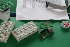
Best Practices for RF Circuit Board Assembly
RF Circuit Board Assembly
The sensitivity of RF circuit boards to interference and noise underscores the need for rigor in design and manufacturing processes. These boards must be able to operate across wide frequency ranges, and the best practices for assembly will ensure that they do so without degrading signal quality or performance.
The right material selection will go a long way toward reducing power losses and maintaining consistent impedance over the intended frequency range. rf circuit board must also be designed to provide adequate shielding and thermal management, and they must include appropriate grounding techniques.
Stack-Up: Proper layering will reduce interference and crosstalk, a significant source of signal distortion. It is recommended that RF components be placed on top of the board and non-RF elements be placed on the lower layers. Each RF layer should have its own dedicated ground plane to provide a short and low-impedance current return path.
Best Practices for RF Circuit Board Assembly
Trace Design: High-frequency signals demand particular attention to trace design. Using microstrip instead of stripline, minimizing the length of traces to minimize attenuation, avoiding parallel placement of RF and standard traces, and optimally bending traces are just some of the important considerations. Via Design: Vias are essential for interconnection, but they can introduce parasitic capacitance when the diameter and layout are not properly controlled. Minimizing vias, ensuring dimensional consistency, and deploying techniques like ground plane stitching can reduce these effects.
Passive Layout: Careful passive layout is critical to RF PCB design. Orienting inductors and capacitors perpendicular to their attached traces, utilizing a flood ground fill around all passives, and implementing vendor 3D or EM-based parasitic models will all help to improve the overall quality of the circuit.
At their core, RF circuit boards are designed to handle signals within the radio frequency spectrum, typically ranging from a few kilohertz to several gigahertz. This spectrum encompasses a wide range of applications, from simple AM/FM radios to sophisticated cellular networks and satellite communication systems.
The design and fabrication of RF circuit boards require careful attention to detail due to the unique characteristics of high-frequency signals. Unlike traditional digital or analog circuitry, RF signals are susceptible to various forms of interference, including parasitic capacitance, inductance, and radiation. As a result, RF circuit boards employ specialized materials, layout techniques, and components to minimize signal loss and maintain signal integrity.
Impedance Matching: In a multi-layer RF PCB, the varying impedances of traces and transmission lines can have a significant impact on the performance of a circuit. Impedance matching is the process of adjusting and matching these varying impedances to achieve stable and efficient performance.
An RF circuit board is an essential piece of technology that transmits and receives radio signals between devices. RF modules are used in a variety of applications, from consumer electronics to automotive and medical equipment. Choosing the right RF circuit board assembly provider will ensure that your products are built to the highest possible standards.