Can Rigid Flex Rigid PCBs Bend Without Damage?
Rigid Flex Rigid PCBs Bend Without Damage
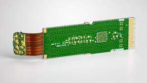
Rigid flex rigid pcbs can be used for medical devices, wearable technology, aerospace systems, and other products that need to bend, flex, or fold. They can also provide greater signal layer density than traditional rigid boards and reduce package size and weight. However, it is important to consider the advantages and disadvantages of rigid flex PCBs and to ensure that they meet the requirements of your design.
When designing a rigid flex PCB, there are several common reliability problems to avoid, including broken copper traces and cracked vias. The first step to avoiding these issues is to make sure that the flexible sections of your circuit have adequate bend radius. This will prevent the formation of sharp, pointed turns that can cause stress on conductor paths and resulting damage. It is also helpful to stagger traces rather than having them overlap each other, as this can help distribute the stress.
Another important consideration is to ensure that the rigid-flex transition area has sufficient clearance between components. Failure to do so can lead to mechanical stress concentration, which can result in copper trace tearing and signal integrity issues. The solution to this is to extend the flex-to-rigid coverlay or bondply into the rigid section of the board, which will provide a seamless transition between the two areas and improve reliability.
Can Rigid Flex Rigid PCBs Bend Without Damage?
Additionally, rigid flex rigid pcb should be pre-baked before assembly to eliminate the risk of moisture absorption, which can delaminate the layers of the board. This is especially important for high-reliability applications, where the PCB must withstand extreme environments and repeated bending.
In addition to addressing the above concerns, it is essential to ensure that your rigid-flex PCB is designed for manufacturability. To do this, you should work closely with your CM to establish the manufacturing and testing processes that are best suited for your design. This will allow you to avoid DFM mistakes that can impact performance, cost, and quality.
Some common DFM mistakes include placing a via in the flex section of the circuit, which can increase manufacturing costs and decrease reliability. To avoid this, you should ensure that your flex section has a minimum of a 10 mil drill-to-copper distance and use a cross-hatched ground plane to minimize stress on the copper traces.
Insufficient tolerances can also lead to a variety of issues, including stacked traces and mechanical stress that leads to thinning of the flex copper. To avoid this, you should ensure that flex traces have adequate widths and pitch and that your stiffeners are not located too close to pins or vias. Using an intuitive CAD tool like Altium Designer can help you avoid these DFM errors and make sure your rigid flex rigid pcbs are ready for production. It can even simulate the bending angles of your flex sections to make sure that they will fit in your mechanical enclosure. To learn more, click the link below.